With the rapid development of wide-bandgap semiconductor materials, silicon carbide (SiC) has become a core material for power electronics and radio frequency (RF) devices due to its excellent thermal stability, high breakdown field strength, and high electron mobility. However, SiC wafers are prone to warping during manufacturing and processing, which not only affects the uniformity of epitaxial growth but also poses challenges to device fabrication and packaging. Therefore, a thorough understanding of the causes, measurement methods, and control strategies for SiC substrate warp is crucial for improving device performance and production yield.
1. Causes of SiC Substrate Warp
The warp of SiC substrates is mainly caused by internal stress, mechanical processing stress, and temperature gradients during thermal processing. The key factors include:
(1) Internal Stress
Thermal Stress: SiC has a highly anisotropic coefficient of thermal expansion (CTE). When wafers undergo drastic temperature changes during growth, processing, or epitaxy, thermal stress develops, leading to warping.
Lattice Defects: Crystal defects such as threading screw dislocations (TSDs), threading edge dislocations (TEDs), and basal plane dislocations (BPDs) introduce localized lattice distortions, contributing to warp.
Doping Stress: The doping process (e.g., n-type doping with nitrogen, p-type doping with aluminum) alters the lattice parameters, generating additional stress that leads to warping.
(2) Mechanical Processing Stress
Grinding and Polishing Stress: Excessive mechanical grinding or chemical mechanical polishing (CMP) can cause residual stress accumulation, resulting in wafer warp.
Epitaxial Layer Stress: The lattice mismatch or thermal expansion mismatch between the epitaxial layer and the substrate—particularly in thick epitaxial layers (>10 µm)—induces additional stress, leading to warp.
(3) Temperature Gradients During Processing
SiC wafers undergo high-temperature treatments (1200-1700°C) during epitaxy and device fabrication. Uneven temperature distribution or rapid cooling rates can create non-uniform thermal stress, contributing to warping.
2. Measurement Methods for SiC Substrate Warp
To accurately evaluate SiC wafer warp, high-precision measurement techniques are required. The commonly used methods include:
| Measurement Method | Principle | Characteristics |
| Optical Interferometry |
Measures wafer topography via light wave interference |
Non-contact, high precision (<1 µm), suitable for large wafers |
| Laser Confocal Scanning | Uses laser scanning to calculate overall wafer warp | Fast, effective for various surface roughnesses |
|
Stylus Profilometry
|
Scans wafer surface with a probe to measure shape variations |
Contact method, ideal for localized warp analysis |
| X-ray Diffraction (XRD) |
Determines lattice distortion via X-ray diffraction |
Useful for analyzing stress-induced warp |
Warp is typically expressed in terms of total warp (Warp) and bow curvature (Bow):
Total Warp: The deviation between the highest and lowest points on the wafer, measured in micrometers (µm).
Bow: The overall curvature of the wafer relative to an ideal plane.
3. Strategies for Controlling SiC Substrate Warp
To reduce SiC substrate warp and enhance device fabrication reliability, several optimization strategies can be implemented.
(1) Optimizing SiC Substrate Processing
Implement low-pressure precision grinding to minimize residual stress during grinding.
Utilize multi-step chemical mechanical polishing (CMP) to gradually remove surface stress layers and improve wafer flatness.
Select appropriate crystallographic orientations (C-plane, A-plane, R-plane, M-plane) to optimize stress distribution.
(2) Controlling SiC Epitaxial Growth Parameters
Optimize epitaxial layer thickness and doping gradients to minimize stress accumulation.
Use graded buffer layers to reduce lattice mismatch stress between the epitaxial layer and the substrate.
Ensure uniform temperature distribution in the chemical vapor deposition (CVD) reactor to prevent large thermal gradients during epitaxy.
Adjust the ratio of SiH₄ (silane) to C₃H₈ (propane) to improve epitaxial layer quality.
(3) Annealing Treatments
High-Temperature Hydrogen Annealing (1600-1800°C): Reduces residual stress and improves wafer flatness.
Slow Cooling Process: Gradual cooling (10-20°C/min) after epitaxy or annealing minimizes thermal stress buildup.
4. Industry Standards for SiC Wafer Warp
Different wafer sizes have specific warp tolerance requirements. The common industry standards are:
6-inch (150 mm) SiC Wafers:
Total Warp < 20 µm (high-quality device grade)
Bow < 10 µm (high uniformity requirement)
8-inch (200 mm) SiC Wafers:
Warp < 30 µm (target level)
Bow < 15 µm (device manufacturing requirement)
5. Conclusion
SiC substrate warp significantly impacts epitaxial layer quality and device performance. The primary causes include internal stress, mechanical processing stress, and thermal gradients during high-temperature processes. By optimizing grinding and polishing processes, refining epitaxial growth parameters, implementing suitable doping strategies, and applying high-temperature annealing treatments, SiC wafer warp can be effectively minimized, leading to high-quality wafers that meet the stringent requirements of power electronics applications. As SiC devices continue to expand into electric vehicles, photovoltaic inverters, and high-frequency communication systems, reducing SiC substrate warp will be a critical factor in enhancing product competitiveness.
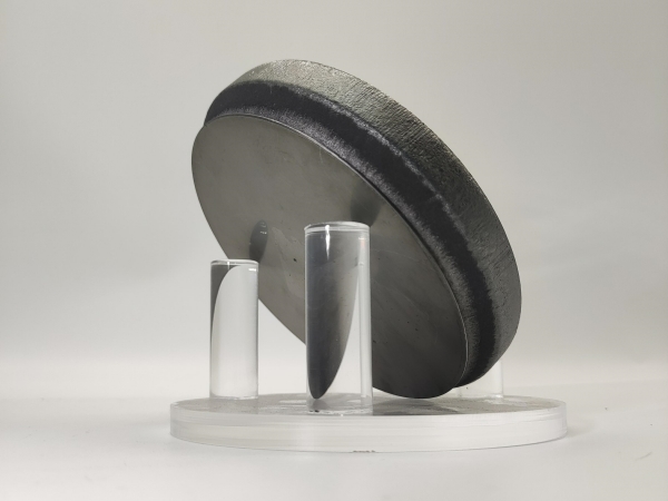
Our SiC substrate products are manufactured with stringent warp control, providing high-quality SiC wafers that maintain Warp values below industry standards, ensuring their suitability for high-end applications.
As semiconductor technology advances, Gallium Nitride (GaN) has become a core material i...
With the rapid advancement of third-generation semiconductor technologies, Silicon Carbi...
As third-generation semiconductor materials such as silicon carbide (SiC) and gallium ni...