As semiconductor technology advances, Gallium Nitride (GaN) has become a core material in optoelectronics, radio frequency (RF) communication, and power devices due to its excellent electrical and optical properties. Among these, GaN-on-Sapphire epitaxial wafers have become the mainstream choice for manufacturing blue LEDs, lasers, ultraviolet (UV) detectors, and other high-performance devices due to their cost-effectiveness and mature processing technology.
Material Advantages: A Strong Partnership Between GaN and Sapphire
Gallium Nitride is a wide-bandgap semiconductor with the following characteristics:
Wide Bandgap (~3.4 eV)
High Electron Mobility
High Breakdown Electric Field Strength
Sapphire (Al₂O₃), as an ideal substrate material for GaN epitaxy, also offers outstanding advantages in both performance and industry maturity:
1. High Mechanical Strength: Suitable for large-wafer preparation and mass production
2. Excellent Optical Transparency: Outstanding transmission from ultraviolet to near-infrared wavelengths
3. Good Thermal Stability: Adapts well to high-temperature processing environments
4. Cost-Effective and Mature Supply Chain: Offers greater market competitiveness compared to SiC and Si substrates
Although there is about a 13.8% lattice mismatch between GaN and sapphire, high-quality GaN epitaxial structures can still be obtained by introducing low-temperature AlN or GaN buffer layers and optimizing the epitaxial process. This meets the performance requirements of most optoelectronic devices.
Epitaxial Structure Diagram:

Process Features: Precise Control and High-Quality Assurance
Epitaxial Method: Metal-Organic Chemical Vapor Deposition (MOCVD)
Dislocation Density Control: Threading Dislocation Density (TDD) controlled between 10⁸~10⁹ cm⁻²
Surface Roughness: As low as sub-nanometer level
Doping and Layer Thickness Control: Achieves high uniformity and device adaptability
Core Application Areas
1. Blue/White LED Chips: The largest and most mature application market globally
2. UV LEDs and Detectors (UV-A/B/C): Widely used in medical, sterilization, and environmental monitoring
3. Laser Diodes (LD): Suitable for laser projection, optical storage, and high-speed optical communications
4. RF Devices (HEMT): Commercial potential for medium- and low-power RF devices
5. Optoelectronic Integrated Chip Platforms: Driving the development of miniaturized and integrated optoelectronic systems
Future Optimization Directions
Although GaN-on-Sapphire epitaxial wafers face challenges such as high dislocation density and poor thermal conductivity, the industry is continuously improving product performance through the following approaches:
Optimizing buffer layer design and stress management techniques
Introducing epitaxial transfer technology (such as transferring to SiC or copper)
Expanding uniformity control capabilities for large sizes (6-inch and above)
Why Choose JXT’s GaN-on-Sapphire?
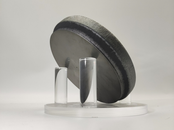
JXT offers high-quality GaN-on-Sapphire epitaxial wafers, available in 2-4 inch sizes, with custom thickness, doping types, and structural designs.
We utilize mature MOCVD epitaxial processes to ensure consistency and high standards in defect density, crystal quality, and surface smoothness for each wafer.
Applications Include:
LED Chip Manufacturing | UV Sensors | Lasers | RF Communication Modules | Optoelectronic Integrated Devices| UV Sensors | Lasers | RF Communication Modules | Optoelectronic Integrated Devices
Flexible Delivery Cycle | Reliable Quality | Custom Development Support| Reliable Quality | Custom Development Support
As semiconductor technology advances, Gallium Nitride (GaN) has become a core material i...
With the rapid advancement of third-generation semiconductor technologies, Silicon Carbi...
As third-generation semiconductor materials such as silicon carbide (SiC) and gallium ni...